Know-how down to the smallest detail
We supply high-tech from the Odenwald. At our Buchen site, we have continuously expanded our vertical range of manufacture over many years. In addition to the heart of our production, the screen printing shop, we are particularly proud of our own electronics production and our optical bonding area. We have all the technologies on offer in-house. This means we can reduce dependencies and have full control over your product quality.
With broad and deep specialist knowledge, many years of experience from countless customer projects and comprehensive industry know-how, we are on hand to advise our customers in every phase of the project.
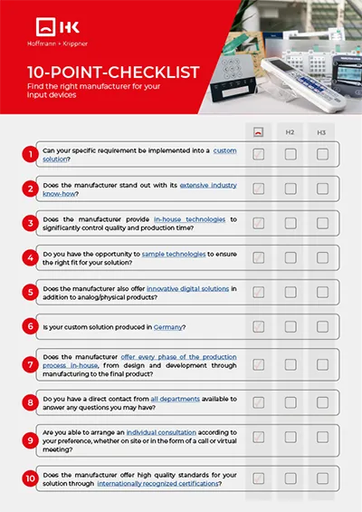
Use our 10-point checklist to compare different manufacturers of input systems and find the right supplier for your requirements.
Construction
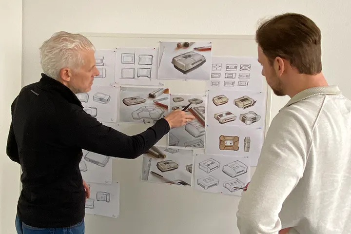
We support you in transforming unfinished ideas into marketable products. Our expert designers and engineers realize individual assemblies or complete HMI solutions, depending on the scope of the project. We use 2D and 3D CAD programs for this purpose. Even if your input system does not yet exist. With the help of photorealistic 3D rendering, we visualize shapes and functions for you down to the smallest detail.
To turn an idea into a finished product, we select the appropriate assembly and production technologies during the design phase. We first test the design of complex operating units in a test setup. The aim here is to combine the diverse requirements with the technical possibilities.
- Development and design of assemblies and complete solutions
- Feasibility check and advice
- Prototype construction
- Design in 3D and 2D CAD
Electronics development
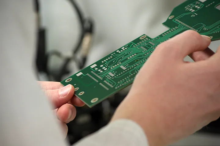
In addition to optimum mechanics and a perfect design, we also develop the associated electronics and software for your input system. According to your requirements, we realize electronic circuits, develop PCB layouts, select durable components and implement individual interfaces. The close proximity to our own electronics production facility enables close cooperation with short coordination channels and fast responses.
In addition to hardware development, we also advise and support you in the development of suitable embedded and application software. We adapt the scope of performance of the electronic unit to the respective area of application and user requirements. That is why it is very important for us to be involved in your development process right from the start. This allows us to make optimum use of our know-how and experience to create the right human-machine interface.
- In-house electronics and software development
- Circuits, PCB layouts, component selection, interfaces
- Close coordination with internal electronics production
- Support for embedded and application software
3D printing (additive manufacturing)
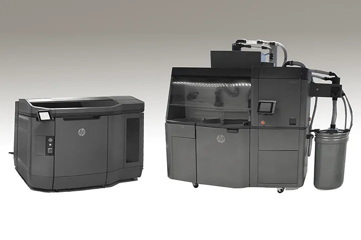
We rely on the HP Multi Jet Fusion process for 3D printing. The innovative Multi Jet Fusion process combines the strengths of the two well-known rapid prototyping processes: Polyjet and Selective Laser Sintering (SLS).
We use additive manufacturing not only for prototypes, but increasingly also for medium and smaller series. Especially for components with a high degree of customization or particularly complicated geometries, 3D printing definitely comes into its own as an optimal alternative or even supplement to the tried-and-tested processes. Take advantage of the benefits of 3D printing:
- Quick and easy implementation
- Only STEP data required, no tools
- Part optimization through function integration
- High customization
Screen printing
Screen printing is at the heart of our production. We have been using this printing process since our company was founded in 1973. The custom designs of our customers are printed on polyester films as well as on glass. To this day, screen printing impresses with its extremely long ink durability, reliable reproducibility and high flexibility in material printing.
We use digital computer-to-screen imaging to create the print template on the screen. Thanks to the CTS process, we no longer need films. The digital data of the print image is exposed directly onto the coated screen via laser exposure. This allows us to position the printed image precisely and means less masking work. Design changes can be implemented quickly thanks to digital screen exposure.
- Very high quality, no pixels visible
- Good reproducibility and weather resistance
- Suitable for larger quantities
- Custom colors can be realized without problems
Electronics assembly
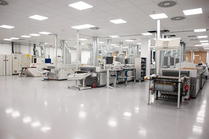
In addition to mechanical assemblies, we also supply the right electronics for your input system. We manufacture your individual electronic solutions in our own SMD assembly with reflow and selective soldering technology. To achieve optimum soldering results, we jet our solder paste directly onto the circuit board. Naturally in compliance with all ESD requirements. Our electronics production is designed to be flexible so that quantities from small to large series can be scaled more easily.
Every electronic unit passes through our test field, where we use our own optical and electronic test concepts to ensure our high quality standards. In addition to our quality promise in accordance with ISO 9001 and safe processes for manufacturing your medical devices in accordance with ISO 13485, we are also happy to support you with individual qualifications.
- Assembly of printed circuit boards and LEDs on foil (FR LEDs)
- Solder paste printing by jet process
- Reflow and selective soldering
- Washing and lacquering of printed circuit boards
- Machine loading of snap domes
Optical Bonding
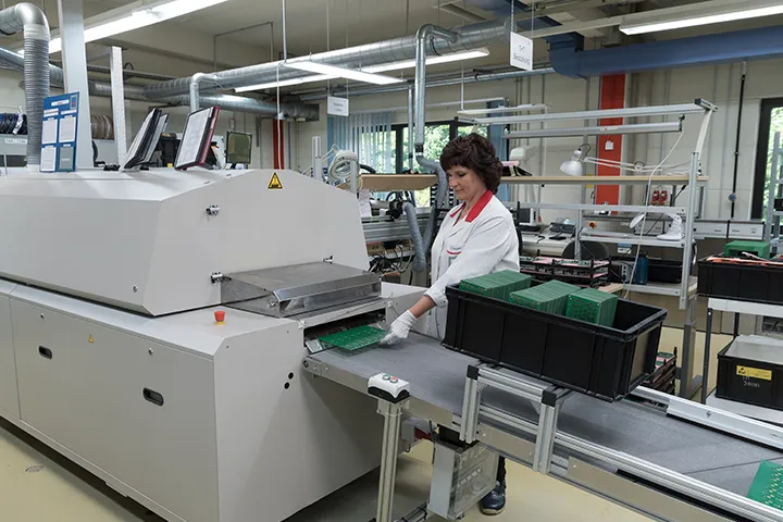
With optical bonding, we combine touch sensors, displays and cover glasses to improve readability in the display area and create a robust input system. We use two different bonding techniques for this: LOCA and OCA. Both bonding processes take place in our production facility under clean room conditions. We use special air-conditioning technology, airlocks and protective clothing to ensure consistently high quality. When it comes to highly transparent adhesives, we rely on sheet and liquid adhesives from well-known brand manufacturers.
Our specially developed systems for the gluing and joining process are freely programmable. We manufacture the necessary tools ourselves. This allows us to respond flexibly to our customers’ requirements and implement individual solutions effectively.
- LOCA and OCA bonding technology in use
- Process takes place in the clean room
- Bonding and joining systems developed in-house
Cut, laser and punch
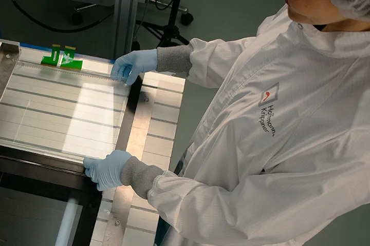
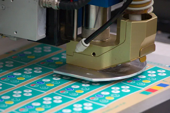
We manufacture the majority of all assemblies in the panel. Several identical layouts are placed on one sheet of film, for example. After the assemblies have passed through all the production steps, the production panel is separated. In the cutting room, the products are cut from large sheets of film to the actual outer contour.
Various processes are available depending on customer requirements. As a rule, larger quantities are punched with the steel rule cutting tool. This is because separation with a single punching process is fast and effective. Our plotters or mirror lasers are used for smaller quantities or smaller dimensional tolerances.
- Die-cut with steel rule cutting tools (for larger quantities or larger tolerances)
- Laser plotting (for smaller quantities or tolerances up to +/- 0.1 mm)
- Mirror laser (for smallest radii and geometries, tolerances up to +/- 0.1 mm)
- Cutting plots (for smaller quantities or tolerances up to +/- 0.1 mm)
Qualifications
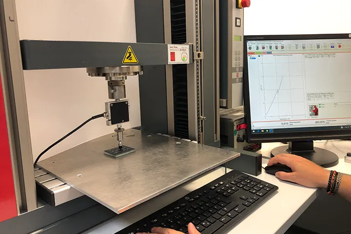
From development to production, we always keep an eye on customer requirements. In addition to our quality assurance in accordance with ISO 9001 and 13485 for medical devices, we also support you with individual qualifications. Various test methods are available in our laboratory for this purpose. Among other things, we test material properties, climatic changes, adhesive durability and the number of switching cycles of our installed contact springs. We also carry out ball drop tests to check the impact resistance of touch systems and displays.
We are familiar with the requirements of many different industries and technologies and draw on this wealth of knowledge to provide you with comprehensive advice. If we cannot cover your desired qualification in-house, we will of course support you in commissioning an external testing laboratory.
- In-house test laboratory
- Service life tests and adhesive pull-off tests
- Climate change tests and temperature shock tests
- Hammer impact test according to DIN EN 62262 (ball drop test)
IP protection concepts
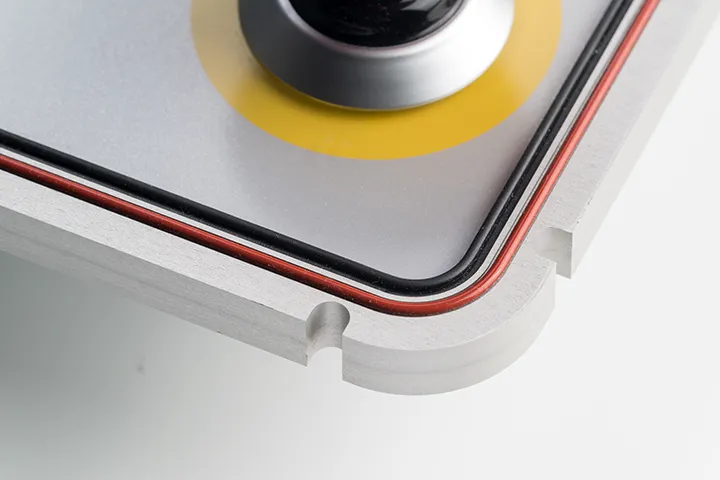
We develop solution concepts for our customers that are specially tailored to their areas of application: From splash-proof membrane keypads to IP65 to HMIs that can even withstand high-pressure cleaning to IP69K. We derive appropriate measures and production processes for this in our design and development department. We pay attention to sufficient bonding and sealing and use reliable materials in the various assemblies.
With our in-house dispensing machine, various sealing materials can be applied to carrier parts, displays or glass in individual contours. Even double beads or EMC gaskets are possible. We use silicone-containing, silicone-free or conductive sealing materials for this purpose. Black, white and transparent seals are available for the front seal. In addition to our dispensed gaskets, we also offer bonded gaskets.
- Development of individual protection and sealing concepts
- Protection class up to IP69K possible
- Dispenste silicone-containing, silicone-free or conductive seals
- Glued foam rubber seals
Quality management
We rely on high-quality materials and reliable processes to live up to our “Made in Germany” quality label. This is how we can supply durable products of high quality to our customers. That is why our processes are certified in accordance with the DIN EN ISO 9001, 14001 and 13485 standards for medical products.
In addition, we rely on a 100% inspection. Every product undergoes a visual inspection and functional test before it leaves our premises. Each button and each LED is controlled via test software. We also check touch systems and displays using our own test programs or test devices provided by the customer.
- Quality management according to DIN EN ISO 9001
- Environmental management according to DIN EN ISO 14001
- Quality management for medical devices according to DIN EN ISO 13485
- 100% final inspection of each product
